How does HDI PCB enable complex routing?.
HDI PCB enable complex routing
The digital world is becoming increasingly complex, and so are the circuit boards that connect it. High-density interconnections (HDI) allow designers to reduce the size of these boards, resulting in smaller electronic devices and more powerful applications. However, these miniaturized boards require a higher number of layers and more intricate routing than standard PCBs. Fortunately, HDI routing can be made easy with the right design tools and by understanding the basics of HDI manufacturing processes.
An important step in the hdi pcb design process is schematic capture, where the electronic circuit is represented in a graphical format. It’s vital to accurately capture and represent the interconnections between components, allowing for smooth HDI manufacturing.
After the schematic is captured, it must be converted into a board layout that is ready for production. This is where the use of a robust and accurate PCB design software package comes into play. A good tool will provide an intuitive user interface and automated design rules, allowing the designer to create a highly efficient layout in no time at all.
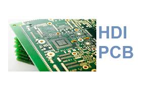
How does HDI PCB enable complex routing?.
The next crucial step in the HDI PCB manufacturing process is to create the layer stack-up and microvias. These are the key technologies that enable high-density routing, and they are created using a combination of two methods: microvia drilling and sequential lamination.
Microvia formation involves laser drilling and plating, creating connections between the layers of the circuit board. Unlike traditional vias that are created after the layers are stacked together, these tiny holes are drilled through the individual layers before the layer build-up is completed.
To ensure that the holes have a sufficient diameter for the desired conductor width, the metallization processes involved in the HDI manufacturing process are modified. The insulating materials are reduced in thickness, and the copper is plated at much thinner thicknesses than with conventional manufacturing techniques.
As the thickness of the conductive elements and the hole sizes decrease, it becomes challenging to maintain signal integrity and electromagnetic interference (EMI) performance. This is where the importance of good CAD tools comes into play, as they need to be capable of modeling the interaction between these layers and the surrounding structures to ensure optimal performance.
The most important thing to understand about the HDI manufacturing process is that there are many different via styles and constructions. The choice of which one to utilize will depend on the design requirements of the circuit board. This includes factors such as the ball pitch of BGA components and the manufacturer’s fabrication capabilities. It’s also essential to verify the manufacturer’s DFM guidelines to avoid wasting material and money.
Choosing the correct via construction is not an easy task. It requires a thorough understanding of the fabrication process, including how vias contribute to densities and how they can be optimized for specific designs. In addition, it’s necessary to understand the impact of drill-to-copper clearance on the overall board reliability. This is where a good PCB design software suite is critical, as it will help the designer to choose the best construction style for each specific design.